Alva Fu¹, Stephen Duan¹ ², Ethan Zhu¹
Abstract. BitVM3 optimizes off-chain verification of SNARK proofs on Bitcoin by replacing Delbrag’s symmetric encryption in garbled circuits (GC) with RSA-based homomorphic encryption. This eliminates the need for costly zero-knowledge proofs to verify entire GC correctness and removes Delbrag’s single-use constraint. In this work, we further enhance BitVM3 by introducing a reusable circuit garbling scheme, which addresses the bottleneck of excessive off-chain data—slashing requirements by 3–4 orders of magnitude (from terabytes to megabytes)—making the solution economically viable. Additionally, we implement several other optimizations: a forward-pass GC generation flow to halve per-gate data, enabling unlimited reuse of GC off-chain data, and formalizing the protocol. These collectively resolve prior scalability issues while maintaining compact on-chain transactions
Keywords: BitVM3, garbled circuits, verification on Bitcoin, layer 2
BitVM3[1] extends BitVM2[2]’s optimistic computation model—which assumes operators are hon- est unless challengers submit fraud proofs on Bitcoin—by leveraging Garbled Circuits (GC)[3] for encrypted-state computations.
Delbrag pioneered the use of Yao’s GC for SNARK(Groth16) verifier while enabling efficienton-chain verification of circuit correctness. The Garbler, acting as an operator in BitVM, constructsa GC and performs the following Protocol:
Delbrag significantly reduces on-chain overhead: assertion transactions are ˜ 100kB, while disproval transactions are merely 32 bytes—a 1,000× cost reduction compared to BitVM2. However, Delbrag’s classical symmetric encryption for GC construction incurs substantial off-chain burdens:
BitVM3 improves Delbrag[5] by replacing symmetric encryption with RSA. Leveraging RSA’s multiplicative homomorphism, it constructs homomorphic GC circuits where intermediate/output labels retain exponentiation properties when input labels are raised to a power. This enables a “reblinding” technique: one set of labels validates circuit correctness, while a ZKP proves commit- ted on-chain input/output labels maintain homomorphic relationships—indirectly ensuring valid GC construction without ZKP verification. Key advantages include:
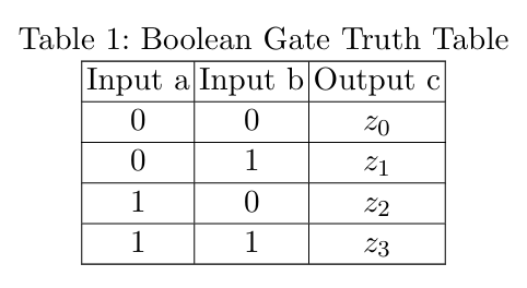
The truth table of a Boolean gate can be represented in Table 1, where \(z_i\) denotes a single-bit value 0 or 1.
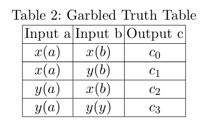
For input wires \(a\) and \(b\), their \(0/1\) labels are denoted \(x(a)/y(a)\) and \(x(b)/y(b)\) (if they are initial circuit inputs, the labels are randomly generated; if they are intermediate values, they are computed from previous gates).
The Garbler selects and publishes an RSA modulus \(N = p \times q\) with secret primes \(p, q\) and public exponents: \(e, e_1, e_2, e_3, e_4\) (invertible modulo \(\phi(N)\)). Output labels are computed using the formula from Bit VM3 below. This approach differs from the Bit VM3 protocol, where output labels are used to compute input labels, whereas our method calculates output labels directly from input labels.
\[\begin{align*}c_0 &= x(a)^e \cdot x(b)^{e_1} \pmod N \\c_1 &= x(a)^e \cdot y(b)^{e_2} \pmod N \\c_2 &= y(a)^e \cdot x(b)^{e_3} \pmod N \\c_3 &= y(a)^e \cdot y(b)^{e_4} \pmod N\end{align*}\]
Obtaining the truth table expressed with labels in Table 2.
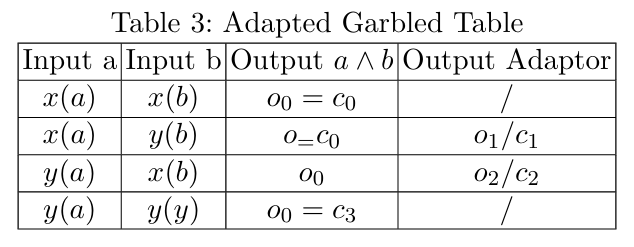
We then introduce output adaptors to unify the output labels of a gate, enforcing that each gate outputs two labels. Let \(o_0, o_1\) be the first output label among \(c_0, c_1, c_2, c_3\) corresponding to plaintext 0 and 1 respectively. For other 0 ciphertexts and 1 ciphertexts, normalize them to \(o_0\) and \(o_1\), respectively:
For all gates that are neither constant 0 nor constant 1, two output adaptors are needed to unify the output labels. Through two output adaptors, we can obtain the final truth table with labels(outputs labels expressed only usingo 0 ando 1 ). Taking gate AND as an example, the final truth table of adapted garbled table is shown in Table 3:
When verifying computation correctness via GC on Bitcoin, the Garbler (i.e., Prover) reveals input labels corresponding to valid inputs, enabling the Evaluator (i.e., Verifier) to execute the GC circuit and derive output labels. If the derived labels mismatch the expected output, this indicates prover fraud.
Unlike traditional GC applications of protecting input plaintext, verification on Bitcoin requires public disclosure of the 0/1 semantics for committed input/output labels. During GC evaluation, the Evaluator always knows the plaintext values of each gate’s input labels, thus determining adaptor usage to adjust output labels while tracking their plaintext meanings. Concurrently, the Garbler must avoid exposing both labels of any input wire to prevent the Evaluator from computing adversarial output labels that trigger penalties.
For a 2-input GC gate, we denote:
The output adaptors are public. Given input labels \( z(a) \in \{x(a), y(a)\} \) and \( z(b) \in \{x(b), y(b)\} \) (revealed by the Garbler or computed from prior gates), the Evaluator:
For the single-input NOT gates, the Garbler requires no cryptographic computation during GC construction—only semantic inversion of label meanings (0→1, 1→0) for subsequent gates. TheEvaluator similarly performs semantic inversion during evaluation. Consequently, NOT gates are free in our GC construction (no cryptographic operations or extra data needed).
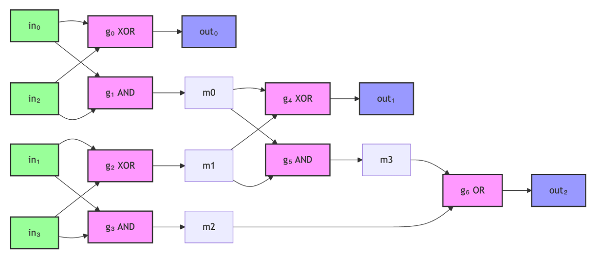
We demonstrate multi-gate composition in a GC circuit using a 2-bit adder example.
Given inputs \((in_0, in_1), (in_2, in_3)\), representing values:
\[a = 2 \cdot in_1 + in_0, \quad b = 2 \cdot in_3 + in_2\]
The 3-bit output \((out_2, out_1, out_0)\) represents:
\[4 \cdot out_2 + 2 \cdot out_1 + out_0 = a + b\]
Example: \((1,0)+(1,1)=(1,0,1)\) encodes \(2+3=5\).
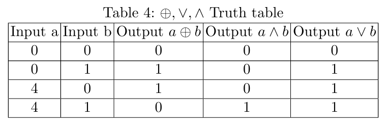
We will use the following three binary gates: XOR \(\oplus\), AND \(\land\), OR \(\lor\) in Table 4.
A 2-bit adder can be constructed using seven gates \(g_0\) to \(g_6\) with the Boolean circuit diagram shown in Figure 1.
The Garbler constructs the GC of the above 2-bit addition.
First, the Garbler generates two random values (labels) for each input bit \(in_0, in_1, in_2, in_3\):
\[x(in_0), y(in_0), x(in_1), y(in_1), x(in_2), y(in_2), x(in_3), y(in_3).\]
Then the Garbler calculates gate-by-gate using the calculating formulas and output adaptor rules. Let \(a_0(g), a_1(g)\) represent the two output adaptors corresponding to gate \(g\).
A GC is described through input labels, output adaptors for all gates and output labels. Given a set of input labels for 2-bit adder: \(z(in_0), z(in_1), z(in_2), z(in_3)\) (\(z = x\) or \(y\), 1 label for each variable),
the Evaluator can use all the output adaptors of the circuit gates to perform the computation and obtain a set of output labels: \(z(out_0), z(out_1), z(out_2)\).
Simulate \(2 + 3 = 5\): using input labels \(x(in_0), y(in_1), y(in_2), y(in_3)\), evaluating the circuit derives output labels \(y(out_0), x(out_1), y(out_2)\).
Adapters can align input labels between GC or sub-GC circuits. When applied to input labels of circuit/sub-circuit, such adapters are termed input adaptors.
Consider two GC/sub-GC circuits with their respective input labels, output adaptors, and output labels denoted as \((L, A, O)\) and \((L', A', O')\). Using the input adaptor \(B = L/L'\), the input labels \(L'\) can be transformed into \(L\), yielding the GC circuit \((L, A, O)\). This conversion leverages the homomorphic properties of GC construction to reuse portions of the circuit description, thereby reducing communication complexity.
GC construction with input adaptors. Consider a Boolean circuit \(C\) that repeatedly invokes sub-circuits \(C_i, i = 1, 2, \cdots, n\), where each \(C_i\) is called \(k_i\) times.
Now, the Garbler first chooses \(k_i\) rebinding factors \(u_{i,j}\) for sub-circuits \(C_i\). Given input labels \(L\), the Garbler constructs the GC with the following two modifications:
We clarify that only the input labels of reused sub-circuits are adjusted. When these labels are used as inputs to other gates in the circuit, they remain unchanged.
GC Description. Now the new GC description comprises:
GC Evaluation. Though we omit detailed description of the GC tuple \((L'_{i,j}, A'_{i,j}, O'_{i,j})\) for the \(j\)-th invocation of \(\mathcal{C}_i\), the input adaptors yield:
\[L'_{i,j} = L_{i,j} \cdot B_{i,j} = L_{i,j}^{u_{i,j}}.\]
Leveraging homomorphic properties in our GC construction – specifically multiplicative/divisional composition of gate labels, output adapters, and input adaptors – we establish:
\[A'_{i,j} = A_{i,j}^{u_{i,j}}, O'_{i,j} = O_{i,j}^{u_{i,j}}.\]
Thus, given \(A, (L_i, A_i, O_i), u_{i,j}, B_{i,j}\), the Evaluator can evaluate the GC with per-bit input labels \(L^* \subset L\), and derive the corresponding per-bit output labels \(O^* \subset O\).
Suppose the Groth16 verification circuit (\mathbb{C}\) repeatedly invokes sub-circuits \(\mathcal{C}_i, i = 1,2, \dots, n\), with each \(\mathcal{C}_i\) being called \(k_i\) times, the Garbler constructs the GC with randomly chosen input labels \( (L, A, (L_i, A_i, O_j)_{i=1,2,\ldots,n}, U_j, B_0) \).
Then the Garbler selects two global reblinding factors (u, v), and:
The GC with input labels \(L^{u}\) is used to verify the consistency of the plaintext, while the GC with input labels \(L^{v}\) constructs an on-chain verification. The validity of committed labels \(L^{v},O^{v}\) is guaranteed by the homomorphic properties between the input-output labels \(L^{u},O^{u}\) and \(L^{v},O^{v}\).
The Evaluator verifies:
Without revealing \(L^v, O^v\), we can ensure the committed \(L^v, O^v\) are consistent with a valid GC and the corresponding output adaptors and input adaptors are \(A^v\) and \(B_{i,j}^v\). When the Garbler reveals a set of valid labels (one for each wire) \(L^* \subset L^v\), the Evaluator can evaluate the GC using output adaptors \(A^v\), input adaptors \(B_{i,j}^v\), and sub-circuit GC \((L_i^v, A_i^v, O_i^v)\), deriving the output labels \(O^* \subset O^v\).
Through choosing a different value \(v\), committing to new input/output labels on Bitcoin, and proposing corresponding ZKP proof about homomorphism between committed input/output labels and \(L^u, O^u\), the scheme can be used again.
The Groth16 verification circuit on the BN254 curve comprises approximately 15 billion gates and executes \(\sim 30,\!000\) modular multiplications. Each modular multiplication operation requires \(\sim 700,\!000\) gates, with RSA modulus of \(256\)-byte. Communication complexity is analyzed as follows:
On-chain complexity follows BitVM3's analysis: 56kB (revealing a set of committed input labels corresponding to plaintext proof) for 'assertTx' and 256 bytes (output label corresponding to 0 output) for 'disproveTx'.
Off-chain complexity totals \(\sim 8\text{GB}\) dominated by adaptor materials of modular multiplication:
The current 8GB off-chain data requirement remains prohibitively large for large-scale applications. In subsequent versions, we will implement nested reuse of submodules to reduce off-chain data by a factor of 10 to 100.


